I include links to products I think could be useful for my readers. As an Amazon Associate, I earn commission from qualifying purchases.
Introduction
Working with development boards like STM32 Discovery or Nucleo Board is good enough for quickly prototyping a proof of concept or validating an idea. But, at some point, you would want to consider designing your own custom STM32 circuit and building a custom STM32 PCB.
In this post, we will discuss the details of designing and manufacturing such a board with KiCad 6 covering: circuit design, PCB layout, and the manufacturing process while uncovering some PCB design guidelines.
Table of Contents
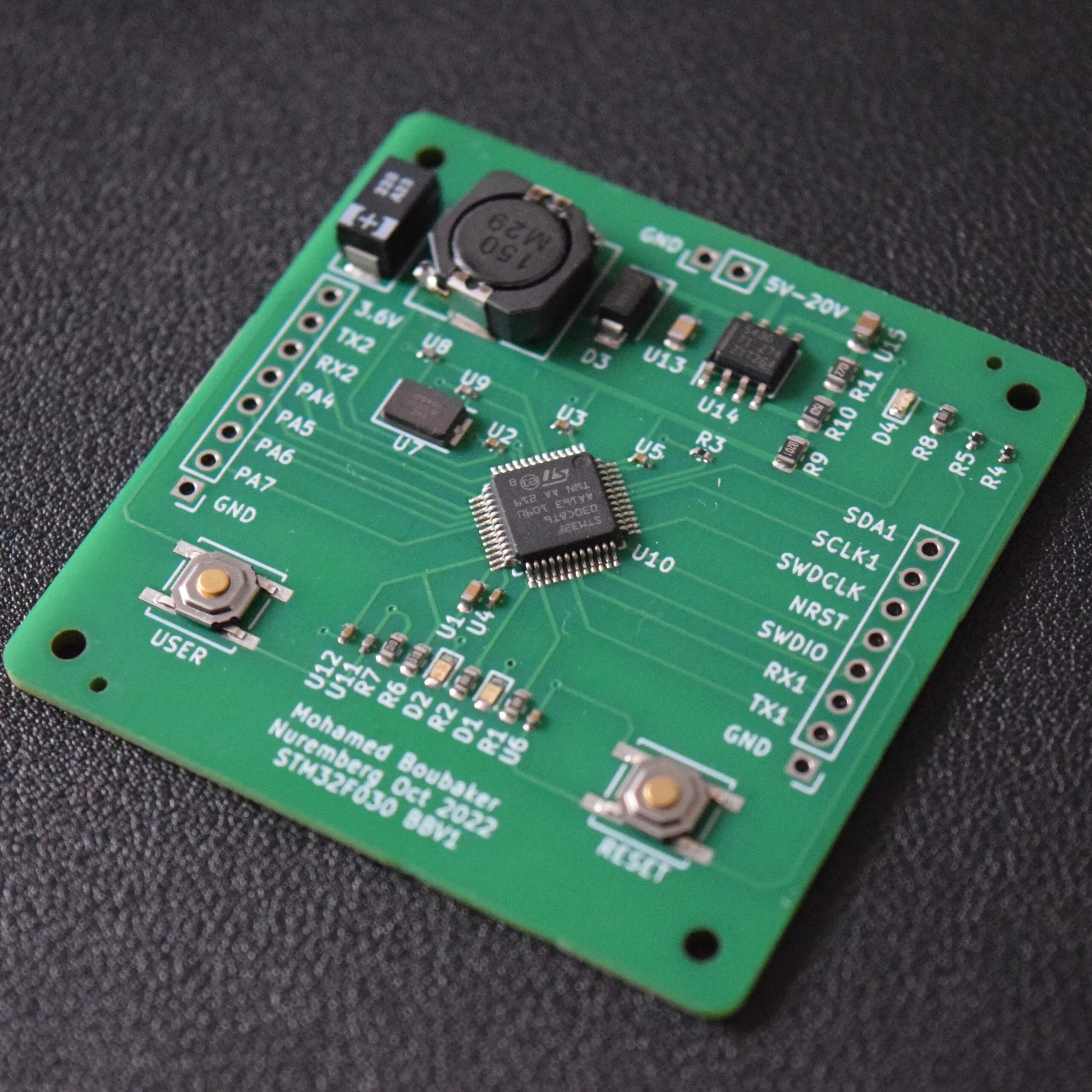
The board features:
- 2 user LEDs.
- DC-DC down converter circuit using TI TPS5430DDA.
- A user button and a reset button.
- Exposed GPIO pins including I2C, UART, and SWD pins for flashing and debugging.
This project is a minimalistic proof of concept designed using KiCad and manufactured using JLCPCB. In fact, It is meant to serve as a source of inspiration for creating more advanced designs that involve an STM32 on a custom PCB. In case you are looking for an STM32 development board, I recommend the Nucleo Board below
You can download all the KiCad design and JLCPCB manufacturing files. If you have any questions or remarks please feel free to leave a comment.
Board Design
Circuit Design
The circuit is composed of 2 main parts: a buck converter circuit to regulate voltage and the STM32 MCU circuit.
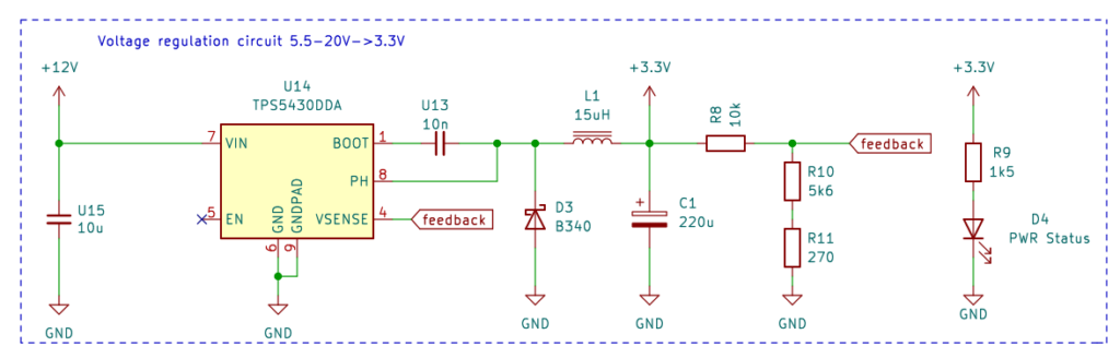
Buck Converter
A voltage regulation circuit using a Texas Instruments TPS5430DDA buck converter configured to provide a stable voltage of 3.6V from any input voltage ranging from 5.5V to 20V. D4 is a red LED that indicates whether the circuit is powered on. All the components surrounding the buck converter and their values are derived from the TPS5430DDA datasheet[1].
To read an in-depth description of the TPS5430DDA circuit check our STM32 GPS Tracker where almost the same circuit is used but with the extra feature of reverse polarity protection and short circuit protection. Below is the schematic for the circuit:
STM32F030 MCU
MCU Specs
The main component of this board is the STM32F030C8T6 MCU running an ARM Cortex-M0 core. This MCU was chosen because of its low cost of $0.7764 and high stock availability. It features:
- 2.4V~3.6V operating voltage
- 4MHz~48MHz clock speed
- 64KB Flash memory
- 8KB SRAM
- 2 USART, 2 I2C and 2 SPI.
- 7 Timers
- 1 ADC
It is suitable for a wide range of applications such as application control, handheld equipment, GPS platforms, alarm systems, sensor nodes, etc.
Below is the circuit surrounding the MCU:
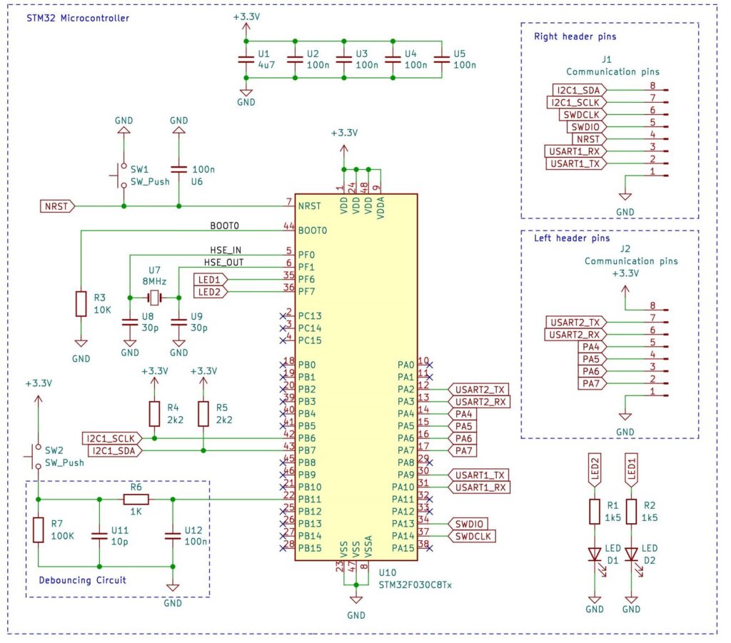
Bypass Capacitors
Capacitors labeled U1, U2, U3, U4, and U5 serve as bypass capacitors, with each of them associated with a VDD pin on the microcontroller, except for U1, which is an additional capacitor. It is recommended to add a 100nF bypass capacitor for each VDD pin plus a global 4.7uF bypass capacitor.
Bypass capacitors are often used to mitigate high-frequency noise originating from the power supply and can also serve as a temporary current reservoir to supply sudden surges of current when needed by the MCU.
Reset Pin NRST
NRST pin is the reset pin and is internally pulled up to VDD. To reset the MCU this pin must be pulled to GND which is done by the push button SW1. The capacitor U6 protects against parasitic resets and according to the datasheet[2] the recommended value is 100nF.
NRST pin is also exposed through pin number 4 of the right header connector J1. To flash and debug the MCU, NRST must be used in conjunction with SWDIO and SWDCLK, and this can be accomplished using the ST-Link programmer or any programmer that supports Serial Wire Debug (SWD)
Serial Wire Debug
During regular operation, PA13 and PA14 function as GPIO pins, but they also have an alternate purpose as SWD signals, specifically SWDIO and SWDCLK, essential for programming the STM32 microcontroller.
To program the MCU, these pins, in addition to the NRST pin, are connected to the ST-LINK programmer like this one
Boot Mode Pin BOOT0
BOOT0 pin helps to select the boot mode. We want the MCU to boot from the main Flash and execute our program. Therefore BOOT0 must be pulled down to GND.
Although the 10KΩ resistor R3 can be omitted, it offers a benefit. If we want to temporarily pull BOOT0 up to VDD to change the boot mode, R3 prevents a short circuit.
Crystal oscillator
PF0 and PF1 connect to the U7 8MHz Crystal oscillator which is surrounded by 2 ceramic capacitors U8 and U9.
LEDs
PF6 is linked to a blue LED labeled D2, while PF7 is connected to a green LED denoted as D1. R1 and R2 help limit the current going through these LEDs. These 2 pins must be configured as output GPIOs to drive the LEDs.
I2C Master
PB6 and PB7 pins are the I2C Master SDA and SCL lines. These 2 pins must not be configured as GPIOs but rather as I2C master. R4 and R5 are the pull-up resistors for the I2C bus. Determining the optimal values of these resistors depends on the line capacitance but a typical value is 2.2KΩ.
UARTs
PA9 and PA10 are the USART1 TX/RX pins. PA2 and PA1 are the USART2 TX/RX pins.
They can be configured as USART ports or can also be configured as GPIOs. They are exposed to the outside through the onboard pin connector.
To communicate with the custom board through UART you need a USB-to-UART adapter like this one:
User Push Button
PB11 is serving as a user input. It is connected to a typical debouncing circuit. The exact circuit and values are inspired by the debouncing circuit found on the STM32F4 Nucleo board.
GPIOs
PA4 through PA7 are GPIO pins and are exposed through the left pin connector.
PCB Layout
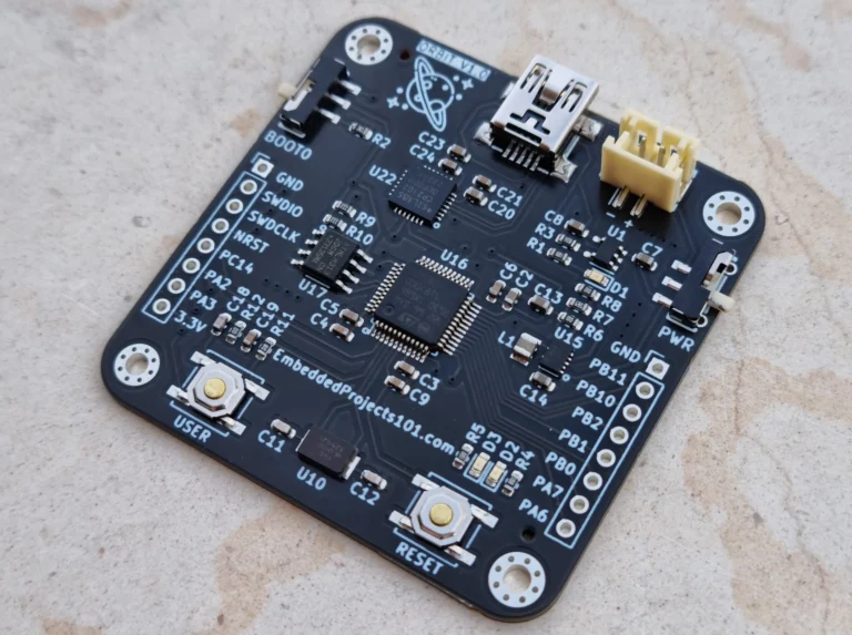
The PCB measures 51x51mm with components placed only on the front side while the back side is just a ground plane.
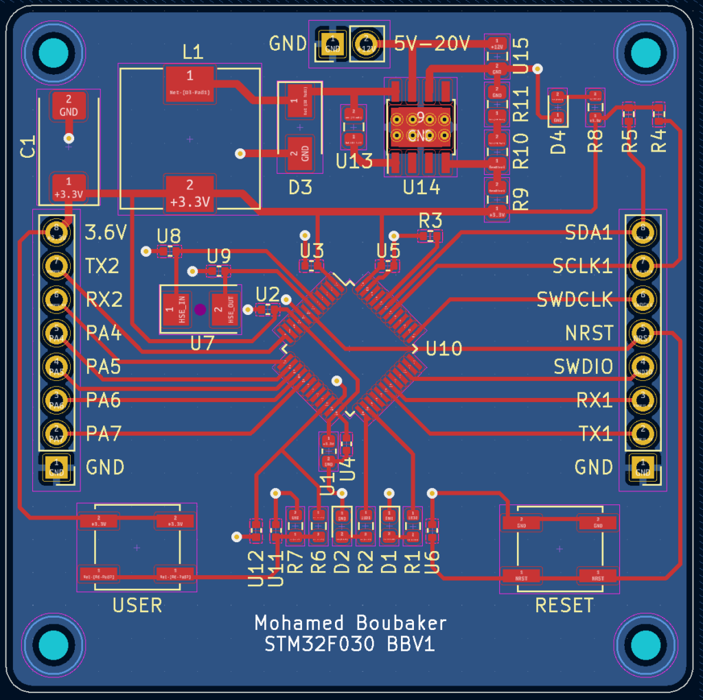
- It’s important to place bypass capacitors close to the MCU. Long traces or leads between the MCU and bypass capacitors can introduce parasitic inductance. By placing the capacitors close, the length of these traces is reduced, which minimizes inductance and ensures that the capacitors can respond quickly to changes in current demand.
- Power-carrying traces should be wider to reduce their resistance hence avoiding any voltage drops that might be caused or any extra heat. KiCad provides the PCB Calculator tool which helps calculate the optimal width for a given PCB trace.
Design Flaws
There are unquestionably opportunities for improvement in this PCB design, as it exhibits certain flaws, most notably:
- Reverse Polarity Protection is missing within the power regulation circuit. This can be achieved by introducing a MOSFET transistor. This shortcoming is addressed in the power regulation circuit of the GPS tracker project.
- Missing BOOT0 switch or jumper. The Boot mode cannot be set as the BOOT0 pin is permanently grounded. There should be a jumper or a switch to set the BOOT0 to VDD or GND.
PCB Manufacturing with JLCPCB
Choosing components
Choosing components is a matter of browsing the JLCPCB parts library and selecting the ones that:
- in stock
- meet power requirements
- have a clear datasheet
- if possible are labeled as “Basic Parts” and not “Extended Parts” because the latter cost 3$ more per component regardless of the component’s price. If you are not careful the extended parts fees can add up quickly.
Below is the list of all the components that were chosen for this PCB, their part numbers, description, and price.
| Component | LSCS Part | Description | Package | Unit Price |
| C1 | C242173 | 220uF 10V 40mΩ@100kHz ±20% | CASE-D-7343 | US$ 0.8903 |
| D1 | C72043 | Emerald 110mW LED | 0603 | US$ 0.0267 |
| D2 | C72041 | Blue 110mW LED | 0603 | US$ 0.0181 |
| D3 | C64982 | 40V 550mV@3A | SMA(DO-214AC) | US$ 0.0331 |
| D4 | C2286 | Red LED | 0603 | US$ 0.0055 |
| L1 | C225048 | 3.5A 15uH ±30% 3.6A | SMD | US$ 0.5553 |
| R1 R2 R8 | C22843 | 1.5kΩ 100mW Thick Film Resistors | 0603 | US$ 0.0010 |
| R10 | C4310 | 1.5kΩ 125mW Thick Film Resistors | 0805 | US$ 0.0018 |
| R11 | C17530 | 2.7kΩ 125mW Thick Film Resistors | 0805 | US$ 0.0017 |
| R3 | C25744 | 10kΩ 62.5mW Thick Film Resistors | 0402 | US$ 0.0005 |
| R4 R5 | C25879 | 2.2kΩ 62.5mW Thick Film Resistors | 0402 | US$ 0.0005 |
| R6 | C21190 | 1kΩ 100mW Thick Film Resistors | 0603 | US$ 0.0006 |
| R7 | C25803 | 100kΩ 100mW Thick Film Resistors | 0603 | US$ 0.0010 |
| R9 | C17828 | 8.2kΩ 125mW Thick Film Resistors | 0805 | US$ 0.0017 |
| SW1 SW2 | C318884 | Tactile Switch | SMD | US$ 0.0155 |
| U1 | C19666 | 16V 4.7uF X5R ±10% | 0603 | US$ 0.0100 |
| U10 | C23922 | STM32F030C8T6 ARM Cortex-M0 | LQFP-48(7×7) | US$ 0.8353 |
| U11 | C32949 | 10pF 50V C0G ±5% | 0402 | US$ 0.0053 |
| U13 | C1710 | 10nF 50V X7R ±10% | 0805 | US$ 0.0070 |
| U14 | C9864 | TI TPS5430DDAR DC-DC Converter | SOP-8 | US$ 0.6046 |
| U15 | C15850 | 25V 10uF X5R ±10% | 0805 | US$ 0.0113 |
| U2 U3 U4 U5 U6 U12 | C1525 | 16V 100nF X7R ±10% | 0402 | US$ 0.0010 |
| U7 | C115962 | Crystal Oscillator 8MHz 20pF | SMD5032-2P | US$ 0.1818 |
| U8 U9 | C1570 | 50V 30pF C0G ±5% | 0402 | US$ 0.0011 |
| US$ 3.2107 |
Generating Manufacturing Files
After finishing the design with KiCad, the last step is to order the assembled PCBs from JLCPCB. To do so, the following design files are required:
- Gerber and Drill files: How to generate Gerber and Drill files in KiCad 7
- BOM and Component Position File: How to generate the BOM and Centroid file from KiCAD
Generating and uploading Gerber files is straightforward, but the BOM and Component position files generated by KiCad are not compatible with the format used by JLCPCB. A small modification must be done before uploading these files to JLCPCB.
Make sure the column names for the BOM csv file are as follows:
Comment,Designator,Footprint,LCSC
For the position csv file, make sure the column names are as follows:
Designator,Value,Footprint,Mid X,Mid Y,Rotation,Layer
You can find more comprehensive explanations of these details in the JLCPCB How-to articles mentioned above.
Results and Evaluation
Programing The Custom Board
There are many IDEs and toolchains to program the STM32 MCUs. For example, ARM Keil, however, it is not free. But it includes a free version for developing on STM32F0 MCUs. There is also the ST-provided STM32CubeIDE and the STM32CubeMX used for MCU configuration and code generation.
After building a program, the outputted hex file must be uploaded into the STM32 Flash memory. For this purpose, the Serial Wire Debug (SWD) programmer below is used.
The SWD interface pins are
- SWDCLK: clock.
- SWDIO: input/output.
- SWDO: it is not available on the STM32F0 family. It is used to print debug messages to the host.
- NRST: reset line.
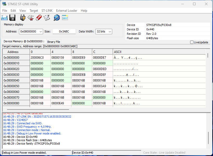
All These 3 pins are exposed through the pin connectors on the PCB. To program the board, these pins need to be connected to the corresponding SWD pins on the ST-LINK programmer. After that, using the ST-LINK Utility the STM32 MCU can be identified and flashed.
Below is a screenshot showing the ST-LINK Utility:
LED Blink Test (Video)
Using STM32CubeMX and STM32CubeIDE a test program to turn on and off GPIO PB12 and PB13 which are connected to the LEDs was created and uploaded to the board using ST-LINK, below is a video showing the result:
Reference and Bibliography
Don’t Miss The Upcoming Projects!
Sign up to the newsletter to get notified whenever a new Project or Tutorial is published.
You can unsubscribe anytime.
The guidance and clarity offered here are highly beneficial for those starting their journey in embedded systems.
keep going 💪