I include links to products I think could be useful for my readers. As an Amazon Associate, I earn commission from qualifying purchases.
Introduction
In this Tutorial, I will explain the functions of the EEPROM pins, how to connect them to the STM32, how to configure the STM32 I2C pins using the STM32CubeMX, and present code examples of using the ST HAL library to perform reads and writes from the STM32 to the EEPROM.
I will also show you how those reads and writes look on the I2C bus using a Logic Analyzer to capture the I2C transactions between the EEPROM and the STM32.
Table of Contents
Prerequisites
First, make sure you have the necessary hardware. For this tutorial, I recommend using an STM32 Nucleo-64 Board and a AT24C256 I2C EEPROM Module.
I assume that you have a working knowledge of how to configure and program an STM32 using STM32CubeMX and STM32CubeIDE and that you are familiar with the STM32 HAL Library
I also suppose you know what an EEPROM is.
Moreover, I assume you have basic knowledge about I2C. But if you don’t, here are some great learning resources: Understanding the I2C Bus from Texas Instruments or this Practical I2C course from Microchip.
EEPROM Pins And Address Configuration
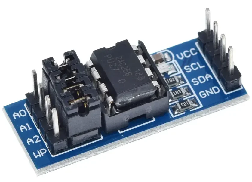
An I2C EEPROM usually comes in an 8-pin package that includes VCC, GND, SDA, SCL, WP, A0, A1, and A2.
SDA and SCL are the Serial Data and Serial Clock of the I2C bus used to connect to the STM32.
WP stands for Write Protect. If WP is connected to VCC then any write operation is ignored. To enable write operations connect WP to GND.
I2C is a Master/Slave bus protocol where each slave has a 7-bit address. In this case, the STM32 is the Master whereas the EEPROM is the slave.
The 7-bit EEPROM I2C Slave address is configurable using the 3 pins A0, A1, and A2. However, it is important to note that when the master addresses a slave on the I2C bus it uses an 8-bit format instead of 7 bits.
- Bit 0 determines if the request from the master is a read or a write; 1 for read, 0 for write.
- Bits 1-3 are called Hardware Client Address and are sampled from pins A0, A1, and A2.
- Bits 4-7 are called Device Type Identifier and are hard-coded into the EEPROM. To find out their value check the EEPROM’s Datasheet. In our case, they are equal to 1010.
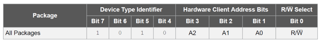
Manipulating A0, A1, and A2 will result in a different address. For example, to program the 7-bit EEPROM address to 0x53 (0101 0011) connect pins A1 and A2 to the VCC and A0 to GND.
How To Connect The STM32 To The EEPROM
If you are using an EEPROM module like the one in the picture above at the beginning of the post, connect the SDA and SCL pins of the STM32 directly to those of the EEPROM.
However, if you are using a bare EEPROM chip, ensure that the I2C signals SDA and SCL are pulled up to VCC using pullup resistors as per the red square in the schematic below.
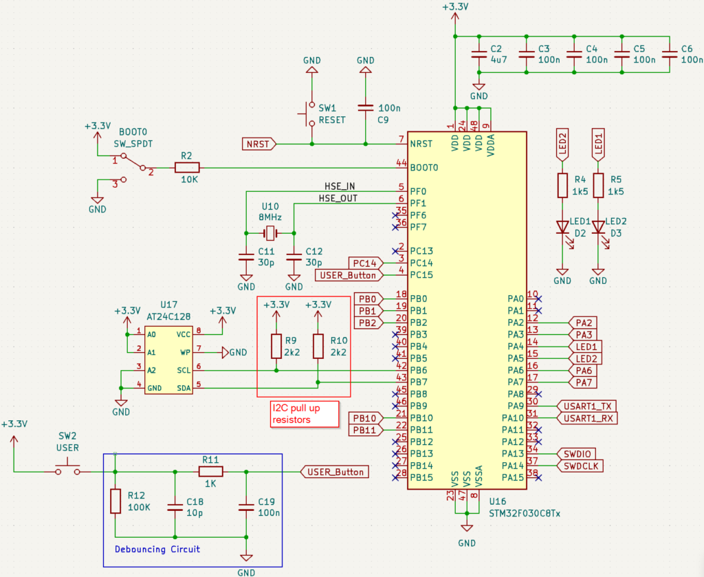
If you want to learn more about the schematic above then check out my other blog post Build a Battery Powered STM32 Board With USB
How To Configure I2C On STM32
Each STM32 model features a varying number of I2C interfaces. Also, the I2C pins, SDA, and SCL can be configured on different pins.
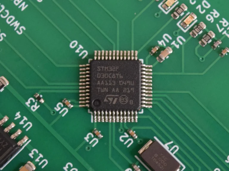
For example, the STM32F411RE that comes with the STM32 Nucleo-64 board includes 3 I2Cs modules. So the first step is to choose one I2C interface and configure its pins.
Configure I2C interfaces using STM32CubeIDE or STM32CubeMX during the early stage of project creation: “Pinout & Configuration” as per the screenshots below.
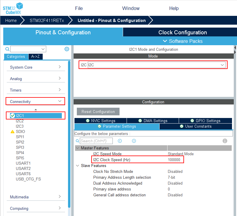
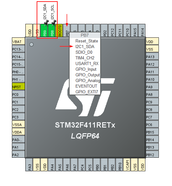
Note that the pins for I2C1 are not limited to PB8 and PB9. You can assign the I2C functionality to different pins by clicking on the pins and choosing the I2C function. For example, PB7 can play the role of I2C1 SDA.
STM32 EEPROM Read Write Code Example
The most important 2 functions to read and write from any I2C slave including an EEPROM are the following:
 HAL_StatusTypeDef HAL_I2C_Mem_Read(
  I2C_HandleTypeDef *  hi2c,
  uint16_t  DevAddress,
  uint16_t  MemAddress,
  uint16_t  MemAddSize,
  uint8_t *  pData,
  uint16_t  Size,
  uint32_t  Timeout
 )
HAL_StatusTypeDef HAL_I2C_Mem_Write(
I2C_HandleTypeDef * hi2c,
uint16_t DevAddress,
uint16_t MemAddress,
uint16_t MemAddSize,
uint8_t * pData,
uint16_t Size,
uint32_t Timeout
) - hi2c Pointer to an I2C_HandleTypeDef structure containing the configuration information for the specified I2C that was configured through STM32CubeMX.
- DevAddress EEPROM I2C address.
Important Note the EEPROM’s 7-bit address value must be shifted to the left by 1 bit before calling this function. As explained in the earlier section “EEPROM pins and address” bit 0 is used by the master to determine the transaction type. - MemAddress Internal EEPROM memory address.
- MemAddSize Size of the internal memory address. For EEPROM, the size is usually 2 bytes.
- pData Pointer to buffer where the data to be read or written is stored.
- Size Amount of data to be read or sent
- Timeout Timeout duration in milliseconds.
Let’s write an example that writes the value 0xEE to the EEPROM with an I2C address of 0x53 at memory address 0x00. If the write is successful, we read back what we wrote.
#define DevAddress 0x53
#define MemAddress 0x00
#define MemAddSize 2
#define Size       1
#define Timeout    100
uint8_t WriteData;
uint8_t ReadData;

WriteData = 0xEE;

HAL_I2C_Mem_Write(&hi2c1, DevAddress << 1, MemAddress, MemAddSize, &WriteData, Size, Timeout);
/* wait utill the write cycle finishes */
HAL_Delay(10);
HAL_I2C_Mem_Read(&hi2c1, DevAddress << 1, MemAddress, MemAddSize, &ReadData, Size, Timeout);
Note how in the example above we shifted the DevAddress to the left by one bit using the shift left operator “<<“.
You should only write up to 64 sequential bytes at a time to the EEPROM, meaning the Size parameter cannot exceed 64.
Internally, the EEPROM writes data in blocks of 64 bytes known as pages. To complete the writing process for each page, the EEPROM needs some time known as the write cycle time (typically around 5 milliseconds).
During the write cycle time, the EEPROM stops listening to the bus until it finishes writing the received bytes. That’s why I waited 10 ms using HAL_Delay(10) right after writing to the EEPROM.
If you write more than 64 bytes in a single write operation, the excess bytes will overwrite the beginning of the same page.
This limitation doesn’t exist for reading, meaning you can read an arbitrary number of bytes at once by changing the function parameter “Size”.
Sniffing I2C EEPROM Transactions With Logic Analyzer
Sometimes, when working with hardware, it’s necessary to examine what’s going on at the signal level. This makes troubleshooting hard-to-catch bugs a breeze.
That’s why, to monitor the I2C Bus activity, I got myself an affordable 24MHz 8-Channel Logic Analyzer like the one below which is compatible with the free open-source Sigrok Pulse View logic analyzer software.
Using Pulse View and the Logic Analyzer I monitored the I2C bus during the write/read operations that we performed in the code example above and captured the 2 screenshots below.
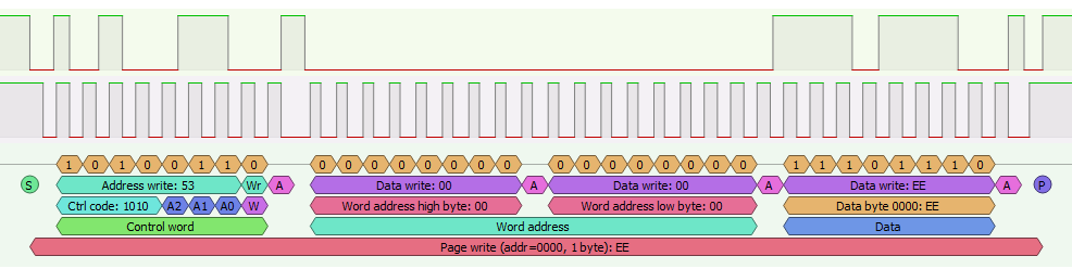
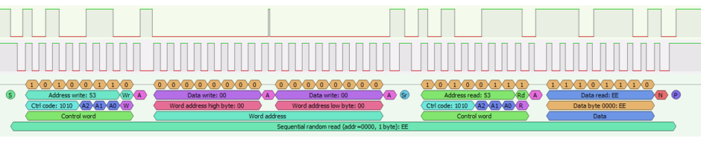
The first signal in both screenshots is SDA and the second is CLK. As for the colored boxes under the signals they are added by the EEPROM protocol decoder feature of Pulse View.
Using the protocol decoder, you can confirm if the slave’s address is correct, or if the slave is replying to the master, and so on.
Don’t Miss The Upcoming Projects!
Sign up to the newsletter to get notified whenever a new Project or Tutorial is published.
You can unsubscribe anytime.